

07 September, 2021


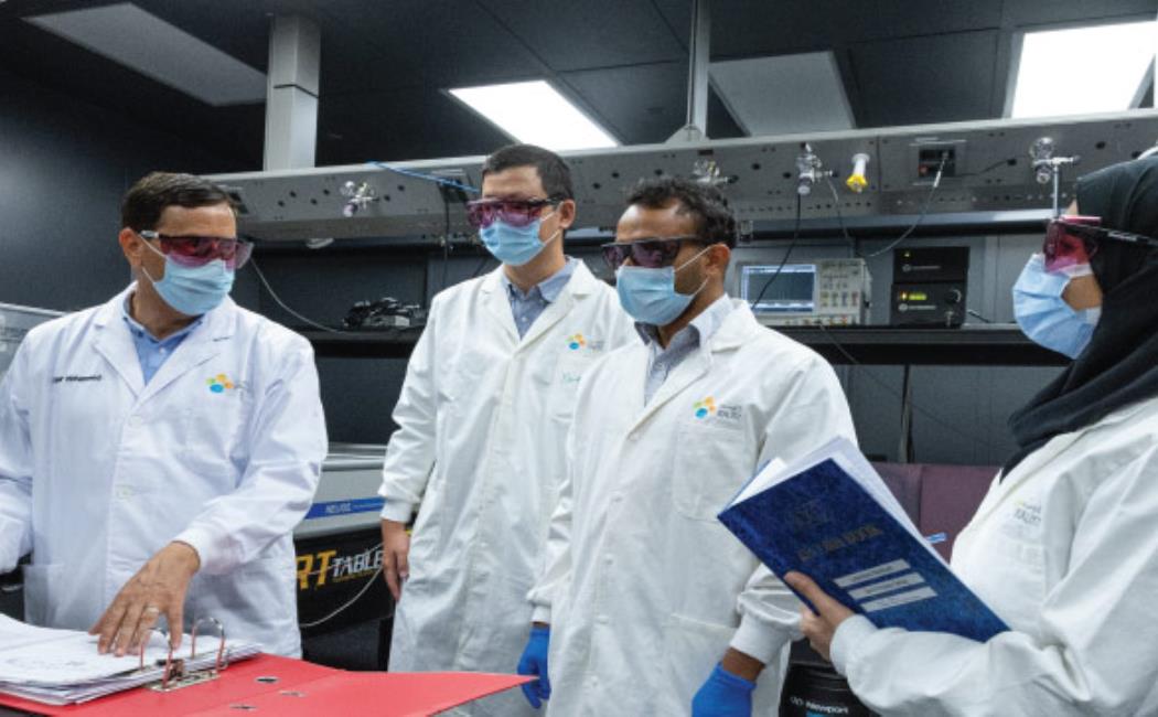
KAUST scientists devise a way to make solar cells more efficient by extending the lifetimes of hot electrons in semiconductors. © 2021 KAUST.
KAUST researchers show that bandgap engineering can improve the performance of optoelectronic devices.
Bandgap engineering can improve the performance of optoelectronic devices that aim to harness the energy of “hot” electrons, research from KAUST shows.
Semiconductors have a signature property known as the bandgap that essentially is a range of forbidden electron energies. Electrons with an energy above the top of the bandgap are free to move through the material, whereas those below the bottom of the bandgap are not, and no electrons with an energy in between can exist in the material.
This simple idea defines a semiconductor’s optical properties. The energy from any absorbed light is transferred to the material’s electrons. Most of the free electrons in a semiconductor have an energy near the top of the bandgap. But the absorption of photons with an energy much larger than the bandgap creates, in turn, much higher energy electrons that are also called “hot electrons.”

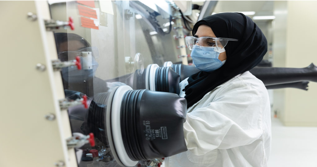
The team designed and fabricated architectures made up of multiple quantum wells: a thin layer of semiconductor sandwiched between light-absorber layers of larger bandgap material. © 2021 KAUST.
Understanding the process by which these so-called hot electrons relax to an energy nearer the top of the bandgap is essential for understanding the operation of light-harvesting devices. For example, the efficiency of a solar cell is reduced if this huge excess energy is lost as heat. “However, it was extremely difficult, if not impossible, to sufficiently utilize these hot electrons in real light-conversion applications due to their very short lifetimes,” says material scientist Omar Mohammed.
Mohammed and his colleagues used interface and bandgap engineering to delay hot carriers (electrons and holes) relaxation and to significantly increase their lifetimes.
The team studied a semiconductor known as a lead halide perovskite. They designed and fabricated architectures made up of multiple quantum wells: a thin layer of semiconductor sandwiched between light-absorber layers of larger bandgap material. They compared the optical properties of structures in which the wells were all the same thickness and asymmetric structures in which the well widths varied. They used a technique called femtosecond (1 femtosecond = 10-15 seconds) transient absorption spectroscopy combined with theoretical calculations to determine the timescale of the hot electron relaxation.

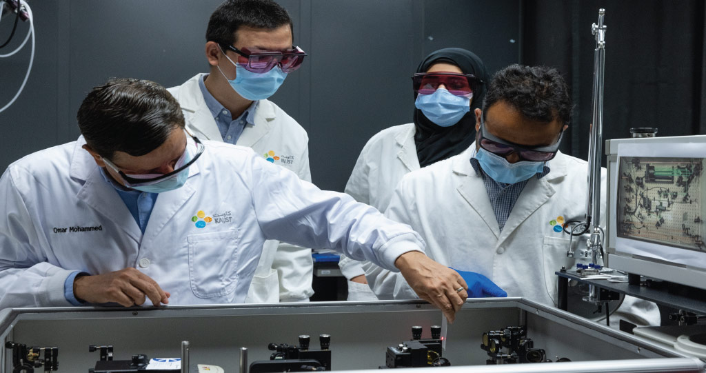
Using a technique called femtosecond transient absorption spectroscopy combined with theoretical calculations, the team could determine the timescale of hot electron relaxation. © 2021 KAUST.
They found the cooling rate had a strong dependence on the quantum well thickness in the asymmetric sample and that the relaxation of the hot carriers in the asymmetric multiple quantum wells was 12.5-fold slower compared to that of the symmetric multiple quantum wells.
“This new finding provides a unique strategy on how to significantly slow down the hot carriers cooling in semiconducting materials for their better utilization in solar cells applications,” says postdoc Partha Maity.
Originally published in
Maity, P., Merdad, N.A., Yin, J., Lee, K. J., Sinatra, L., Bakr, O.M. & Mohammed, O.F. Cascade electron transfer induces slow hot carrier relaxation in CsPbBr3 asymmetric quantum wells. ACS Energy Letters 6, 2602−2609 (2021).| article